Integrated Silicon Solution, Inc. — www.issi.com —
1-800-379-4774
1
Rev. C
04/13/06
IS61LV10248 ISSI
®
Copyright © 2006 Integrated Silicon Solution, Inc. All rights reserved. ISSI reserves the right to make changes to this specification and its products at any time
without notice. ISSI assumes no liability arising out of the application or use of any information, products or services described herein. Customers are advised to
obtain the latest version of this device specification before relying on any published information and before placing orders for products.
1M x 8 HIGH-SPEED CMOS STATIC RAM
APRIL 2006
FEATURES
• High-speed access times:
8, 10 ns
• High-performance, low-power CMOS process
• Multiple center power and ground pins for
greater noise immunity
• Easy memory expansion with CE and OE
options
• CE power-down
• Fully static operation: no clock or refresh
required
• TTL compatible inputs and outputs
• Single 3.3V power supply
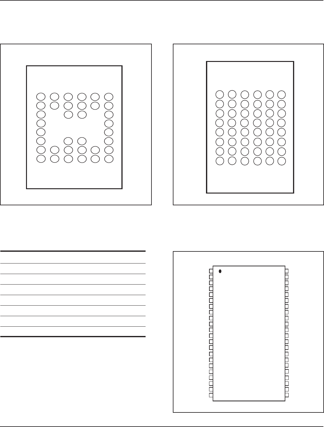
• Packages available:
–
48-ball miniBGA (9mm x 11mm)
– 36-ball miniBGA
(9mm x 11mm)
– 44-pin TSOP (Type II)
• Lead-free available
DESCRIPTION
The ISSI IS61LV10248 is a very high-speed, low power,
1M-word by 8-bit CMOS static RAM. The IS61LV10248 is
fabricated using ISSI's high-performance CMOS technol-
ogy. This highly reliable process coupled with innovative
circuit design techniques, yields higher performance and
low power consumption devices.
When CE is HIGH (deselected), the device assumes a
standby mode at which the power dissipation can be
reduced down with CMOS input levels.
The IS61LV10248 operates from a single 3.3V power
supply and all inputs are TTL-compatible.
The IS61LV10248 is available in 48 ball mini BGA, 36-ball
mini BGA, and 44-pin TSOP (Type II) packages.
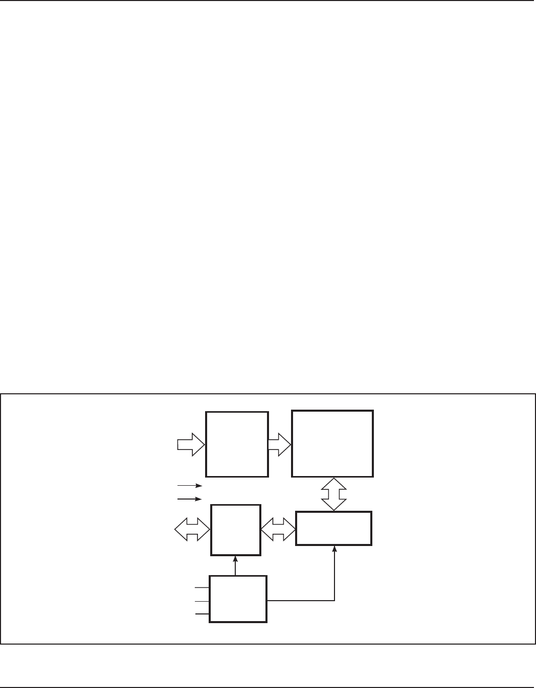
FUNCTIONAL BLOCK DIAGRAM
A0-A19
CE
OE
WE
1M X 8
MEMORY ARRAY
DECODER
COLUMN I/O
CONTROL
CIRCUIT
GND
VDD
I/O
DATA
CIRCUIT
I/O0-I/O7

Integrated Silicon Solution, Inc. — www.issi.com —
1-800-379-4774
3
Rev. C
04/13/06
IS61LV10248 ISSI
®
ABSOLUTE MAXIMUM RATINGS
(1)
Symbol Parameter Value Unit
VTERM Terminal Voltage with Respect to GND –0.5 to VDD + 0.5 V
VDD VDD Relates to GND –0.3 to 4.0 V
TSTG Storage Temperature –65 to +150 °C
PT Power Dissipation 1.0 W
Notes:
1. Stress greater than those listed under ABSOLUTE MAXIMUM RATINGS may cause permanent damage
to the device. This is a stress rating only and functional operation of the device at these or any other
conditions above those indicated in the operational sections of this specification is not implied. Exposure
to absolute maximum rating conditions for extended periods may affect reliability.
TRUTH TABLE
Mode
WEWE
WEWE
WE
CECE
CECE
CE
OEOE
OEOE
OE I/O Operation VDD Current
Not Selected X H X High-Z I
SB1, ISB2
(Power-down)
Output Disabled H L H High-Z ICC
Read H L L DOUT ICC
Write L L X DIN ICC
OPERATING RANGE
Range Ambient Temperature VDD
Commercial 0°C to +70°C 3.3V +10%, -5%
Industrial –40°C to +85°C 3.3V +10%, -5%
CAPACITANCE
(1,2)
Symbol Parameter Conditions Max. Unit
CIN Input Capacitance VIN = 0V 6 pF
CI/O Input/Output Capacitance VOUT = 0V 8 pF
Notes:
1. Tested initially and after any design or process changes that may affect these parameters.
2. Test conditions: T
A = 25°C, f = 1 MHz, VDD = 3.3V.