15815509278
取消

04025A101JAT2A

  • 04025A101JAT2A
  • 04025A101JAT2A
04025A101JAT2A
CAPACITOR
AVX CORPORATION
Cap Ceramic 100
-
YES
4
Typical Capacitance Change
Envelope: 0 ± 30 ppm/°C
% Capacitance
+0.5
0
-0.5
-55 -35
-15 +5 +25 +45 +65 +85 +105
+125
Temperature °C
Temperature Coefficient
Insulation Resistance (Ohm-Farads)
1,000
10,000
100
0
0
20
40 60 80
Temperature °C
Insulation Resistance vs Temperature
100
Impedance,
10
100 1000
Frequency, MHz
Variation of Impedance with Chip Size
Impedance vs. Frequency
1000 pF - C0G (NP0)
1.0
0.1
10
1206
0805
1812
1210
Impedance,
10
100 1000
Frequency, MHz
Variation of Impedance with Ceramic Formulation
Impedance vs. Frequency
1000 pF - C0G (NP0) vs X7R
0805
0.10
0.01
1.00
X7R
NPO
10.00
% Capacitance
+1
+2
0
-1
-2
1KHz
10 KHz 100 KHz 1 MHz 10 MHz
Frequency
Capacitance vs. Frequency
Impedance,
1,000
10,000
100
1
10
100 1000
Frequency, MHz
Variation of Impedance with Cap Value
Impedance vs. Frequency
0805 - C0G (NP0)
10 pF vs. 100 pF vs. 1000 pF
10 pF
100 pF
1000 pF
1.0
0.1
10.0
100,000
C0G (NP0) Dielectric
General Specifications
C0G (NP0) is the most popular formulation of the
“temperature-compensating,” EIA Class I ceramic
materials. Modern C0G (NP0) formulations contain
neodymium, samarium and other rare earth oxides.
C0G (NP0) ceramics offer one of the most stable capacitor
dielectrics available. Capacitance change with temperature
is 0 ±30ppm/°C which is less than ±0.3% C from -55°C
to +125°C. Capacitance drift or hysteresis for C0G (NP0)
ceramics is negligible at less than ±0.05% versus up to
±2% for films. Typical capacitance change with life is less
than ±0.1% for C0G (NP0), one-fifth that shown by most
other dielectrics. C0G (NP0) formulations show no aging
characteristics.
0805
Size
(L" x W")
5
Voltage
6.3V = 6
10V = Z
16V = Y
25V = 3
50V = 5
100V = 1
200V = 2
500V = 7
A
Dielectric
C0G (NP0) = A
101
Capacitance
Code (In pF)
2 Sig. Digits +
Number of
Zeros
J
Capacitance
Tolerance
B = ±.10 pF (<10pF)
C = ±.25 pF (<10pF)
D = ±.50 pF (<10pF)
F = ±1% (≥ 10 pF)
G = ±2% (≥ 10 pF)
J = ±5%
K = ±10%
A
Failure
Rate
A = Not
Applicable
T
Terminations
T = Plated Ni
and Sn
7 = Gold Plated
2
Packaging
2 = 7" Reel
4 = 13" Reel
7 = Bulk Cass.
9 = Bulk
Contact
Factory
For
Multiples
A
Special
Code
A = Std.
Product
PART NUMBER (see page 2 for complete part number explanation)
Contact
Factory For
1 = Pd/Ag Term
NOTE: Contact factory for availability of Termination and Tolerance Options for Specific Part Numbers.
Contact factory for non-specified capacitance values.
5
C0G (NP0) Dielectric
Specifications and Test Methods
Parameter/Test NP0 Specification Limits Measuring Conditions
Operating Temperature Range -55ºC to +125ºC Temperature Cycle Chamber
Capacitance Within specified tolerance Freq.: 1.0 MHz ± 10% for cap ≤ 1000 pF
Q
<30 pF: Q≥ 400+20 x Cap Value 1.0 kHz ± 10% for cap > 1000 pF
≥30 pF: Q≥ 1000 Voltage: 1.0Vrms ± .2V
Insulation Resistance
100,000MΩ or 1000MΩ - μF, Charge device with rated voltage for
whichever is less 60 ± 5 secs @ room temp/humidity
Charge device with 300% of rated voltage for
Dielectric Strength No breakdown or visual defects 1-5 seconds, w/charge and discharge current
limited to 50 mA (max)
Note: Charge device with 150% of rated
voltage for 500V devices.
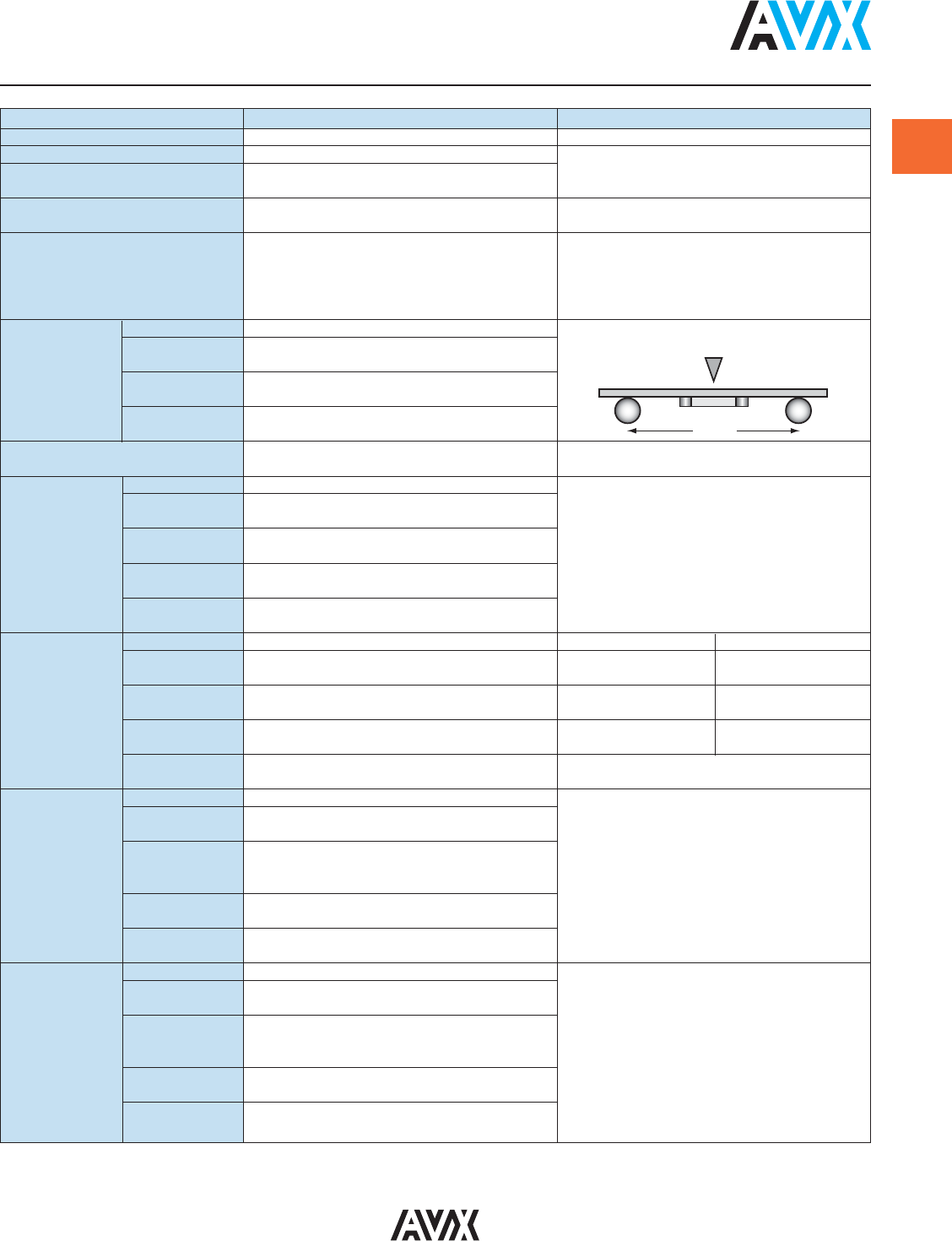
Appearance No defects Deflection: 2mm
Capacitance Test Time: 30 seconds
Resistance to Variation
±5% or ±.5 pF, whichever is greater
Flexure
Q Meets Initial Values (As Above)
Stresses
Insulation
≥ Initial Value x 0.3
Resistance
Solderability
≥ 95% of each terminal should be covered Dip device in eutectic solder at 230 ± 5ºC
with fresh solder for 5.0 ± 0.5 seconds
Appearance No defects, <25% leaching of either end terminal
Capacitance
Variation
≤ ±2.5% or ±.25 pF, whichever is greater
Dip device in eutectic solder at 260ºC for 60
Q Meets Initial Values (As Above)
seconds. Store at room temperature for 24 ± 2
Resistance to
hours before measuring electrical properties.
Solder Heat
Insulation
Meets Initial Values (As Above)
Resistance
Dielectric
Meets Initial Values (As Above)
Strength
Appearance No visual defects Step 1: -55ºC ± 2º 30 ± 3 minutes
Capacitance
Variation
≤ ±2.5% or ±.25 pF, whichever is greater Step 2: Room Temp ≤ 3 minutes
Q Meets Initial Values (As Above) Step 3: +125ºC ± 2º 30 ± 3 minutes
Thermal
Shock
Insulation
Meets Initial Values (As Above) Step 4: Room Temp ≤ 3 minutes
Resistance
Dielectric
Meets Initial Values (As Above)
Repeat for 5 cycles and measure after
Strength 24 hours at room temperature
Appearance No visual defects
Capacitance
Variation
≤ ±3.0% or ± .3 pF, whichever is greater
Charge device with twice rated voltage in
≥ 30 pF: Q≥ 350 test chamber set at 125ºC ± 2ºC
Load Life
Q
≥10 pF, <30 pF: Q≥ 275 +5C/2 for 1000 hours (+48, -0).
(C=Nominal Cap)
<10 pF: Q≥ 200 +10C
Insulation
≥ Initial Value x 0.3 (See Above)
Remove from test chamber and stabilize at
Resistance room temperature for 24 hours
Dielectric
Meets Initial Values (As Above)
before measuring.
Strength
Appearance No visual defects
Capacitance
Variation
≤ ±5.0% or ± .5 pF, whichever is greater
Store in a test chamber set at 85ºC ± 2ºC/
30 pF: Q≥ 350 85% ± 5% relative humidity for 1000 hours
Load Q ≥10 pF, <30 pF: Q≥ 275 +5C/2 (+48, -0) with rated voltage applied.
Humidity <10 pF: Q≥ 200 +10C
Insulation
≥ Initial Value x 0.3 (See Above)
Remove from chamber and stabilize at
Resistance room temperature for 24 ± 2 hours
Dielectric
Meets Initial Values (As Above)
before measuring.
Strength
1mm/sec
90 mm
6
C0G (NP0) Dielectric
Capacitance Range
Letter ABCEGJKMNPQXYZ
Max. 0.33 0.22 0.56 0.71 0.90 0.94 1.02 1.27 1.40 1.52 1.78 2.29 2.54 2.79
Thickness (0.013) (0.009) (0.022) (0.028) (0.035) (0.037) (0.040) (0.050) (0.055) (0.060) (0.070) (0.090) (0.100) (0.110)
PAPER EMBOSSED
SIZE 01005 0201 0402 0603 0805 1206
Soldering Reflow Only Reflow Only Reflow/Wave Reflow/Wave Reflow/Wave Reflow/Wave
Packaging All Paper All Paper All Paper All Paper Paper/Embossed Paper/Embossed
(L) Length
mm 0.40 ± 0.02 0.60 ± 0.03 1.00 ± 0.10 1.60 ± 0.15 2.01 ± 0.20 3.20 ± 0.20
(in.) (0.016 ± 0.0008) (0.024 ± 0.001) (0.040 ± 0.004) (0.063 ± 0.006) (0.079 ± 0.008) (0.126 ± 0.008)
(W) Width
mm 0.20 ± 0.02 0.30 ± 0.03 0.50 ± 0.10 0.81 ± 0.15 1.25 ± 0.20 1.60 ± 0.20
(in.) (0.008 ± 0.0008) (0.011 ± 0.001) (0.020 ± 0.004) (0.032 ± 0.006) (0.049 ± 0.008) (0.063 ± 0.008)
(t) Terminal
mm 0.10 ± 0.04 0.15 ± 0.05 0.25 ± 0.15 0.35 ± 0.15 0.50 ± 0.25 0.50 ± 0.25
(in.) (0.004 ± 0.016) (0.006 ± 0.002) (0.010 ± 0.006) (0.014 ± 0.006) (0.020 ± 0.010) (0.020 ± 0.010)
WVDC 16 25 50 16 25 50 16 25 50 100 16 25 50 100 200 16 25 50 100 200 500
Cap 0.5 A C C C G G G G J J J J J J J J J J J
(pF) 1.0 B A C C C G G G G J J J J J J J J J J J
1.2 B A C C C G G G G J J J J J J J J J J J
1.5 B A A C C C G G G G J J J J J J J J J J J
1.8 B A A C C C G G G G J J J J J J J J J J J
2.2 B A A C C C G G G G J J J J J J J J J J J
2.7 B A A C C C G G G G J J J J J J J J J J J
3.3 B A A C C C G G G G J J J J J J J J J J J
3.9 B A A C C C G G G G J J J J J J J J J J J
4.7 B A A C C C G G G G J J J J J J J J J J J
5.6 B A A C C C G G G G J J J J J J J J J J J
6.8 B A A C C C G G G G J J J J J J J J J J J
8.2 B A A C C C G G G G J J J J J J J J J J J
10 B AACCCGGGGJ J JJ JJ JJ J J J
12 B AACCCGGGGJ J JJ JJ JJ J J J
15 B AACCCGGGGJ J JJ JJ JJ J J J
18 B AACCCGGGGJ J JJ JJ JJ J J J
22 B AACCCGGGGJ J JJ JJ JJ J J J
27 AACCCGG GGJ J JJ JJ JJ J J J
33 AACCCGG GGJ J JJ JJ JJ J J J
39 A CCCGGGGJ J JJ JJ JJ J J J
47 A CCCGGGGJ J JJ JJ JJ J J J
56 A CCCGGGGJ J JJ JJ JJ J J J
68 A CCCGGGGJ J JJ JJ JJ J J J
82 A CCCGGGGJ J JJ JJ JJ J J J
100 A C C C G G G G J J J J J J J J J J J
120 C C C G G G G J J J J J J J J J J J
150 C C C G G G G J J J J J J J J J J J
180 C C C G G G G J J J J J J J J J J J
220 C C C G G G G J J J J J J J J J J M
270 C C C G G G G J J J J M J J J J J M
330 C C C G G G G J J J J M J J J J J M
390 C C C G G G J J J J M J J J J J M
470 C C C G G G J J J J M J J J J J M
560 G G G J J J J M J J J J J M
680 G G G J J J J J J J J J P
820 G G G J J J J J J J J M
1000 G G G J J J J J J J J Q
1200 JJ J J JJJQ
1500 JJ J J JJMQ
1800 JJ J J JMM
2200 JJN J JMP
2700 JJN J JMP
3300 JJ J JMP
3900 JJ J JMP
4700 JJ J JMP
5600 JJM
6800 MM
8200 MM
Cap 0.010 MM
(µF) 0.012
0.015
0.018
0.022
0.027
0.033
0.039
0.047
0.068
0.082
0.1
WVDC 25 50 16 25 50 16 25 50 100 16 25 50 100 200 16 25 50 100 200 500
SIZE 01005 0201 0402 0603 0805 1206
PREFERRED SIZES ARE SHADED

Analog Devices Inc./Maxim Integrated
IC DESERIALIZER GMSL 1.5GBPS
Power Integrations
LQA08TC600 Series 600 V 8 A Through Hole Schottky Diode - TO-220AC
ROHM
DTC144EUA Series 50 V 100 mA Surface Mount NPN Digital Transistor - SC-70
Nexperia
PMEG6010 Series 60 V 9 A Low VF MEGA Schottky Barrier Rectifier - SOD-123F
SMC
MBRF20200 Series 200 V 20 A Through Hole Schottky Rectifier - ITO-220AC
Micro Commercial Components
GBU6J Series 600 v 6 A Through Hole Glass Passivated Bridge Rectifier - GBU-4
Microchip
Operational Amplifier, 1MHz with EMI Filter
HARTING
Circular Metric Connectors M8 D-code PushPull 4pin straight m shielded AWG26-22 for cable 6.2-6.8mm
Microchip
ZL40203 Series 750 MHz Surface Mount Precision 1:4 LVPECL Fanout Buffer - QFN-16
Panasonic
EB-A Series 160 V 33 uF Ø10x20mm LS=5mm 105°C Radial Electrolytic Capacitor
Yageo
RT Series 0805 0.125 W 69.8 kOhm ±0.1% ±50 ppm/°C SMT Thin Film Chip Resistor
Walsin Technology Corporation
WF06U Series 0603 12 Ω 0.063 W ±0.1% ±25 ppm/°C Thin Film Chip Resistor
ROHM
Res Current Sense Metal Plate 2512 0.047 Ohm 1% 3W ±20ppm/°C
API Delevan
Common Mode Chokes / Filters 500uH
Triad Magnetics
C Series 0.035 H -20 to 50 % Tol. 2 A Unshielded Chassis Mount Power Inductor
Analog Devices Inc.
IC DAC 16BIT A-OUT 196CSPBGA
TE Connectivity / Corcom
AC Power Entry Modules 6A DUAL FUSE SNAP IN MOUNT
TE Connectivity / Corcom
AC Power Entry Modules NO FILTER/SNGL FUSE SNAP IN MOUNT
Advantech
DC Power Cords Power Cable VDC 3m
AVX CORPORATION
Cap Ceramic 100pF 50V C0G 5%Pad SMD 0402 125°C T/RAdditional Information:
关闭
Inquiry
captcha

15815509278

295144934@qq.com
0