3D3521
MONOLITHIC MANCHESTER
ENCODER
(SERIES 3D3521)
FEATURES
• All-silicon, low-power CMOS
technology
• 3.3V operation
• CMOS compatible inputs and
outputs
• Vapor phase, IR and wave
solderable
• Auto-insertable (DIP pkg.)
• Low ground bounce noise
• Maximum data rate: 50 MBaud
FUNCTIONAL DESCRIPTION
The 3D3521 is a monolithic CMOS Manchester Encoder. The clock
and data, present at the unit input, are combined into a single bi-phase-
level signal. In this encoding mode, a logic one is represented by a
high-to-low transition within the bit cell, while a logic zero is represented
by a low-to-high transition. The unit operating baud rate (in Mbaud) is
equal to the input clock frequency (in MHZ). All pins marked N/C must
be left unconnected.
a
delay
devices,
inc.
3
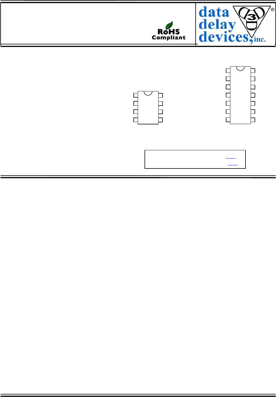
PACKAGES
8
7
6
5
1
2
3
4
CLK
RESB
DAT
GND
VDD
N/C
TXB
TX
3D3521M DIP (.300)
3D3521H Gull Wing (.300)
3D3521Z SOIC (.150)
14
13
12
11
10
9
8
1
2
3
4
5
6
7
CLK
N/C
N/C
RESB
DAT
N/C
GND
VDD
N/C
N/C
N/C
N/C
TXB
TX
3D3521 DIP (.300)
3D3521G Gull Wing (.300)
3D3521D SOIC (.150)
PIN DESCRIPTIONS
DAT Data Input
CLK Clock Input
RESB Reset
TX Signal Output
TXB Inverted Signal Output
VDD +3.3 Volts
GND Ground
For mechanical dimensions, click here.
For package marking details, click here.
The all-CMOS 3D3521 integrated circuit has been designed as a reliable, economic alternative to hybrid
Manchester Encoders. It is CMOS-compatible and is offered in standard 8-pin and 14-pin auto-insertable
DIPs and space saving surface mount 8-pin and 14-pin SOICs.
Doc #06004 DATA DELAY DEVICES, INC. 1
5/8/2006 3 Mt. Prospect Ave. Clifton, NJ 07013

3D3521
APPLICATION NOTES
The 3D3521 Manchester Encoder samples the
data input at the rising edge of the input clock.
The sampled data is used in conjunction with the
clock rising and falling edges to generate the by-
phase level Manchester code.
INPUT SIGNAL CHARACTERISTICS
The 3D3521 Manchester Encoder inputs are
CMOS compatible. The user should assure
himself that the 50% (of VDD) threshold is used
when referring to all timing, especially to the input
clock duty cycle.
CLOCK DUTY CYCLE ERRORS
The 3D3521 Manchester Encoder employs the
timing of the clock rising and falling edges (duty
cycle) to implement the required coding scheme.
To reduce the difference between the output data
high time and low time, it is essential that the
deviation of the input clock duty cycle from 50/50
be minimized.
OUTPUT SIGNAL CHARACTERISTICS
The 3D3521 presents at its outputs the true and
the complimented encoded data.
The High-to-Low time skew of the selected data
output should be budgeted by the user, as it
relates to his application, to satisfactorily
estimate the distortion of the transmitted data
stream.
Such an estimate is very useful in determining
the
functionality and margins of the data link, if a
3D3522 Manchester Decoder is used to decode
the received data.
POWER SUPPLY AND
TEMPERATURE CONSIDERATIONS
CMOS integrated circuitry is strongly dependent
on power supply and temperature. The
monolithic 3D3521 Manchester encoder utilizes
novel and innovative compensation circuitry to
minimize timing variations induced by fluctuations
in power supply and/or temperature.
RESET
(RESB)
CLOCK
(CIN)
DATA
(DIN)
TRANSMIT
(TX)
TRANSMIT
(TXB)
t
DS
t
DH
Figure 1: Timing Diagram
1/f
C
10110010
10110010
Power-on reset (Left high for normal operation)
T
2H
T
2L
T
1H
T
1L
Doc #06004 DATA DELAY DEVICES, INC. 2
5/8/2006 Tel: 973-773-2299 Fax: 973-773-9672 http://www.datadelay.com
3D3521
DEVICE SPECIFICATIONS
TABLE 1: ABSOLUTE MAXIMUM RATINGS
PARAMETER SYMBOL MIN MAX UNITS NOTES
DC Supply Voltage V
DD
-0.3 7.0 V
Input Pin Voltage V
IN
-0.3 V
DD
+0.3 V
Input Pin Current I
IN
-10 10 mA 25C
Storage Temperature T
STRG
-55 150 C
Lead Temperature T
LEAD
300 C 10 sec
TABLE 2: DC ELECTRICAL CHARACTERISTICS
(-40C to 85C, 3.0V to 3.6V)
PARAMETER SYMBOL MIN MAX UNITS NOTES
Static Supply Current* I
DD
5 mA
High Level Input Voltage V
IH
2.0 V
Low Level Input Voltage V
IL
1.0 V
High Level Input Current I
IH
1.0
µA
V
IH
= V
DD
Low Level Input Current I
IL
1.0
µA
V
IL
= 0V
High Level Output Current I
OH
-4.0 mA V
DD
= 3.0V
V
OH
= 2.4V
Low Level Output Current I
OL
4.0 mA V
DD
= 3.0V
V
OL
= 0.4V
Output Rise & Fall Time T
R
& T
F
2 ns C
LD
= 5 pf
*I
DD
(Dynamic) = 2 * C
LD
* V
DD
* F Input Capacitance = 10 pf typical
where: C
LD
= Average capacitance load/pin (pf) Output Load Capacitance (C
LD
) = 25 pf max
F = Input frequency (GHz)
TABLE 3: AC ELECTRICAL CHARACTERISTICS
(-40C to 85C, 3.0V to 3.6V)
PARAMETER
SYMBOL
MIN TYP MAX UNITS NOTES
Input Baud Rate f
BN
50 MBaud
Clock Frequency f
C
50 MHz
Data set-up to clock rising t
DS
3.5 ns
Data hold from clock rising t
DH
0 ns
TX High-Low time skew t
1H
- t
1L
-3.5 3.5 ns 1
TXB High-Low time skew t
2H
- t
2L
-2.0 2.0 ns 1
TX - TXB High/Low time skew t
1H
- t
2L
-3.0 3.0 ns 1
Notes: 1: Assumes a 50% duty cycle clock input
Doc #06004 DATA DELAY DEVICES, INC. 3
5/8/2006 3 Mt. Prospect Ave. Clifton, NJ 07013


(LF)(SN).jpg "B18B-PNDZS-1(T)(LF)(SN)")


