1
®
3650/52
3650
3652
Optically-Coupled Linear
ISOLATION AMPLIFIERS
FEATURES
● BALANCED INPUT
● LARGE COMMON-MODE VOLTAGES:
±2000V Continuous
140dB Rejection
● ULTRA LOW LEAKAGE:
0.35
µA max at 240V/60Hz
1.8pF Leakage Capacitance
● EXCELLENT GAIN ACCURACY:
0.05% Linearity
0.05%/1000 Hrs Stability
● WIDE BANDWIDTH:
15kHz
±3dB
1.2V/µs Slew Rate
APPLICATIONS
● INDUSTRIAL PROCESS CONTROL
● DATA ACQUISITION
● INTERFACE ELEMENT
● BIOMEDICAL MEASUREMENTS
● PATIENT MONITORING
● TEST EQUIPMENT
● CURRENT SHUNT MEASUREMENT
● GROUND-LOOP ELIMINATION
● SCR CONTROLS
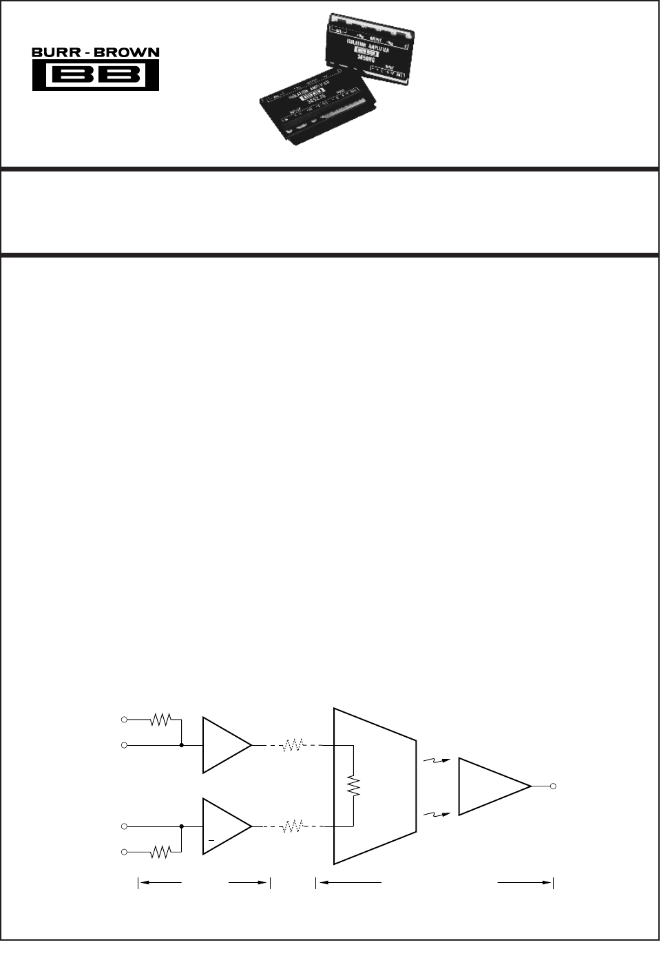
DESCRIPTION
The 3650 and 3652 are optically coupled integrated
circuit isolation amplifiers. Prior to their introduction
commercially available isolation amplifiers had been
modular or rack mounted devices using transformer
coupled modulation demodulation techniques.
Compared to these earlier isolation amplifiers, the
3650 and 3652 have the advantage of smaller size,
lower cost, wider bandwidth and integrated circuit
reliability. Also, because they use a DC analog modu-
lation technique as opposed to a carrier-type tech-
nique, they avoid the problems of electro-
magnetic interference (both transmitted and received)
that most of the modular isolation amplifiers exhibit.
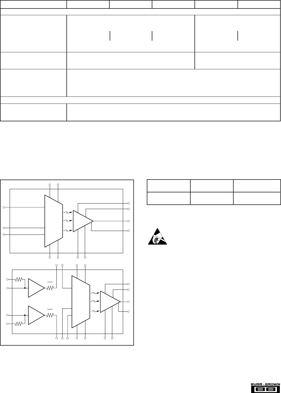
A
1
A
1
11
10
8
9
Light
Flux
Coupling
23
A
3
A
4
1.6MΩ
1.6MΩ
R
G1
R
G2
R
IN
3652 Only Common to 3650 and 3652
3
1
6
4
®
International Airport Industrial Park • Mailing Address: PO Box 11400, Tucson, AZ 85734 • Street Address: 6730 S. Tucson Blvd., Tucson, AZ 85706 • Tel: (520) 746-1111 • Twx: 910-952-1111
Internet: http://www.burr-brown.com/ • FAXLine: (800) 548-6133 (US/Canada Only) • Cable: BBRCORP • Telex: 066-6491 • FAX: (520) 889-1510 • Immediate Product Info: (800) 548-6132
©
1976 Burr-Brown Corporation PDS-342L Printed in U.S.A. August, 1997
SBOS129
2
®
3650/52
SPECIFICATIONS
At +25°C and ±15VDC supply voltages, unless otherwise specified.
10
6
10
6
R
G1
+ R
G2
+ R
IN
R
G1
+ R
G2
+ R
IN
+ R
O
25Ω
90Ω ±30Ω
PRODUCT 3650MG, HG
(1)
3650JG 3650KG 3652MG, HG
(1)
3652JG
ISOLATION
Isolation Voltage
Rated Continuous, min 2000Vp or VDC
Tested Voltage, min, 10s Duration 5000Vp
Isolation Mode Rejection, G = 10
DC 140dB
60Hz, 5000Ω Source Unbalance 120dB
Leakage Current, 240V/60Hz 0.35µA, max
Isolation Impedance
Capacitance 1.8pF
Resistance 10
12
Ω
GAIN
Gain Equation
for Current Sources G
1
= 10
6
V/Amp G
1
= 1.0057 x 10
6
V/Amp
(2)
for Voltage Sources G
V
1 = V/V V/V
Input Resistance, R
IN
, max 25Ω
Buffer Output Impedance, R
O
Not Applicable
Gain Equation Error, max
(3)
1.5% 0.5% 0.5% 1.5%
(4)
0.5%
(4)
Gain Nonlinearity ±0.05% typ ±0.2% max ±0.03% typ ±0.1% max ±0.02% typ ±0.05% max ±0.05% typ ±0.2% max ±0.05% typ ±0.1% max
Gain vs Temperature 300ppm/°C 100ppm/°C 50ppm/°C 300ppm/°C 200ppm/°C
Gain vs Time ±0.05%/1000hrs ±0.05%/1000hrs
Frequency Response
Slew Rate 0.7V/µs min, 1.2V/µs typ
±3dB Frequency 15kHz
Settling Time
to ±0.01% 400µs
to ±0.1% 200µs
INPUT STAGE
(5)
Input Offset Voltage
at 25°C, max
(3)
±5mV ±1mV ±0.5mV ±5mV ±2mV
vs Temperature, max ±25µV/°C ±10µV/°C ±5µV/°C ±50µV/°C ±25µV/°C
vs Supply 100µV/V 100µV/V
vs Time 50µV/1000hrs 100µV/1000hrs
Input Bias Current
at 25°C 10nA typ, 40nA max 10pA typ, 50pA max
vs Temperature 0.3nA/°C Doubles Every +10°C
vs Supply 0.2nA/V 1pA/V
Input Offset Current 10pA
vs Temperature Effects Included Doubles Every +10°C
vs Supply In Output Offset 1pA/V
Input Impedance
Differential “R
IN
” = 25Ω max 10
11
Ω
Common-Mode 10
9
Ω 10
11
Ω
Input Noise
Voltage, 0.05Hz to 100Hz 4µVp-p 8µVp-p
10Hz to 10kHz 4µVrms 5µVrms
Input Voltage Range
Common-Mode, Linear Operation, ±(|V| –5)V ±(|V| –5)
w/o damage, at +, – ±V ±V
at +I, –I Not Applicable
(6)
±300V for 10ms
(7)
at +I
R
, –I
R
Not Applicable
(6)
±3000V for 10ms
(7)
Differential, w/o damage, at +, – ±V ±V
Differential, w/o damage, at +I, –I Not Applicable ±600V for 10ms
(7)
Differential, w/o damage,
at +I
R
, –I
R
Not Applicable ±6000V for 10ms
(7)
Common-Mode Rejection, 60Hz 90dB at 60Hz, 5kΩ Imbalance 80dB at 60Hz, 5kΩ Imbalance
Power Supply (Input Stage Only)
Voltage (at “+V” and “–V”) ±8V to ±18V ±8V to ±18V
Current
Quiescent ±1.2mA
(8)
±3mA
(8)
with ±10V Output
(7)
+6.5mA or –6.5mA, typ +8.5mA or –8.5mA, typ
+12mA or –12mA, max +16mA, or –16mA, max
3
®
3650/52
A
1
A
2
1.6MΩ
1.6MΩ
R
O
2
R
O
2
Gain Adj Gain Adj
811 13 14
15 1612109 32 29
17
C
23
20
26
6
4
3
1
C
–
+
–V
+V
Bal
+V
CC
–V
CC
Bal
3652
13 14
15 16
10
32 29
17
C
23
20
26
C
–
+
–V
+V
Bal
+V
CC
–V
CC
Bal
3650
12
11
SPECIFICATIONS (CONT)
At +25°C and ±15VDC supply voltages, unless otherwise specified.
PRODUCT 3650MG, HG
(1)
3650JG 3650KG 3652MG, HG
(1)
3652JG
OUTPUT STAGE
Output Voltage, min ±10V ±10V
Output Current, min ±5mA ±5mA
Output Offset Voltage
at 25°C, max
(3)
±25mV ±10mV ±10mV ±25mV ±10mV
vs Temperature, max ±900µV/°C ±450µV/°C ±300µV/°C ±900µV/°C ±450µV/°C
vs Supply ±500µV/V ±500µV/V
vs Time ±1mV/1000hrs ±1mV/1000hrs
Output Noise Voltage
0.05Hz to 100Hz 50µVp-p 50µVp-p
10Hz to 1kHz 65µVrms 65µVrms
Power Supply (Output Stage Only)
Voltage (“+V
CC
” and “–V
CC
”) ±8V to ±18V
Current
Quiescent ±2.3mA typ, ±6mA max
with ±5mA Output, max ±11mA
TEMPERATURE
(9)
Specification 0°c to +85°C
Operating –40°C to +100°C
Storage –40°C to +125°C
NOTES: (1) All electrical and mechanical specifications of the 3650MG and 3652MG are identical to the 3650HG and 3652HG, respectively, except that the following
specifications apply to the 3650MG and 3652MG: (a) Isolation test voltage duration increased from 10 seconds minimum to 60 seconds minimum; (b) Input offset voltage
at 25°C, max: ±10mV; vs temperature max: ±100µV/°C; (c) Output offset voltage at 25°C, max; ±50mV; vs temperature max; ±1.8mV/°C. (2) If used as 3650, see
Installation and Operating Instructions. (3) Trimmable to zero. (4) Gain error terms specified for inputs applied through buffer amplifiers (i.e., ±1 or ±I
R
pins). (5) Input
stage specifications at +I and –I inputs for 3652 unless otherwise noted. (6) Maximum safe input current at either input is 10mA. (7) Continuous rating is 1/3 pulse rating.
(8) Load current is drawn from one supply lead at a time: other supply current at quiescent level. For 3652 add 0.2mA/V of positive CMV. (9) dT/dt < 1°C/minute below
0°C, and long-term storage above 100°C is not recommended. Also limit the repeated thermal cycles to be within the 0°C to +85°C temperature range.
PIN CONFIGURATIONS
PACKAGE INFORMATION
PACKAGE DRAWING
PRODUCT PACKAGE NUMBER
(1)
3650 32-Pin DIP 77
3652 32-Pin DIP 77
NOTE: (1) For detailed drawing and dimension table, please see end of data
sheet, or Appendix C of Burr-Brown IC Data Book.
ELECTROSTATIC
DISCHARGE SENSITIVITY
This integrated circuit can be damaged by ESD. Burr-Brown
recommends that all integrated circuits be handled with
appropriate precautions. Failure to observe proper handling
and installation procedures can cause damage.
ESD damage can range from subtle performance degrada-
tion to complete device failure. Precision integrated circuits
may be more susceptible to damage because very small
parametric changes could cause the device not to meet its
published specifications.
The information provided herein is believed to be reliable; however, BURR-BROWN assumes no responsibility for inaccuracies or omissions. BURR-BROWN
assumes no responsibility for the use of this information, and all use of such information shall be entirely at the user’s own risk. Prices and specifications are subject
to change without notice. No patent rights or licenses to any of the circuits described herein are implied or granted to any third party. BURR-BROWN does not
authorize or warrant any BURR-BROWN product for use in life support devices and/or systems.