CAUTION: These devices are sensitive to electrostatic discharge. Users should follow proper I.C. Handling Procedures.
Copyright
© Harris Corporation 1994
1
SEMICONDUCTOR
CD54AC193/3A
CD54ACT193/3A
Presettable Synchronous
4-Bit Binary Up/Down Counter with Reset
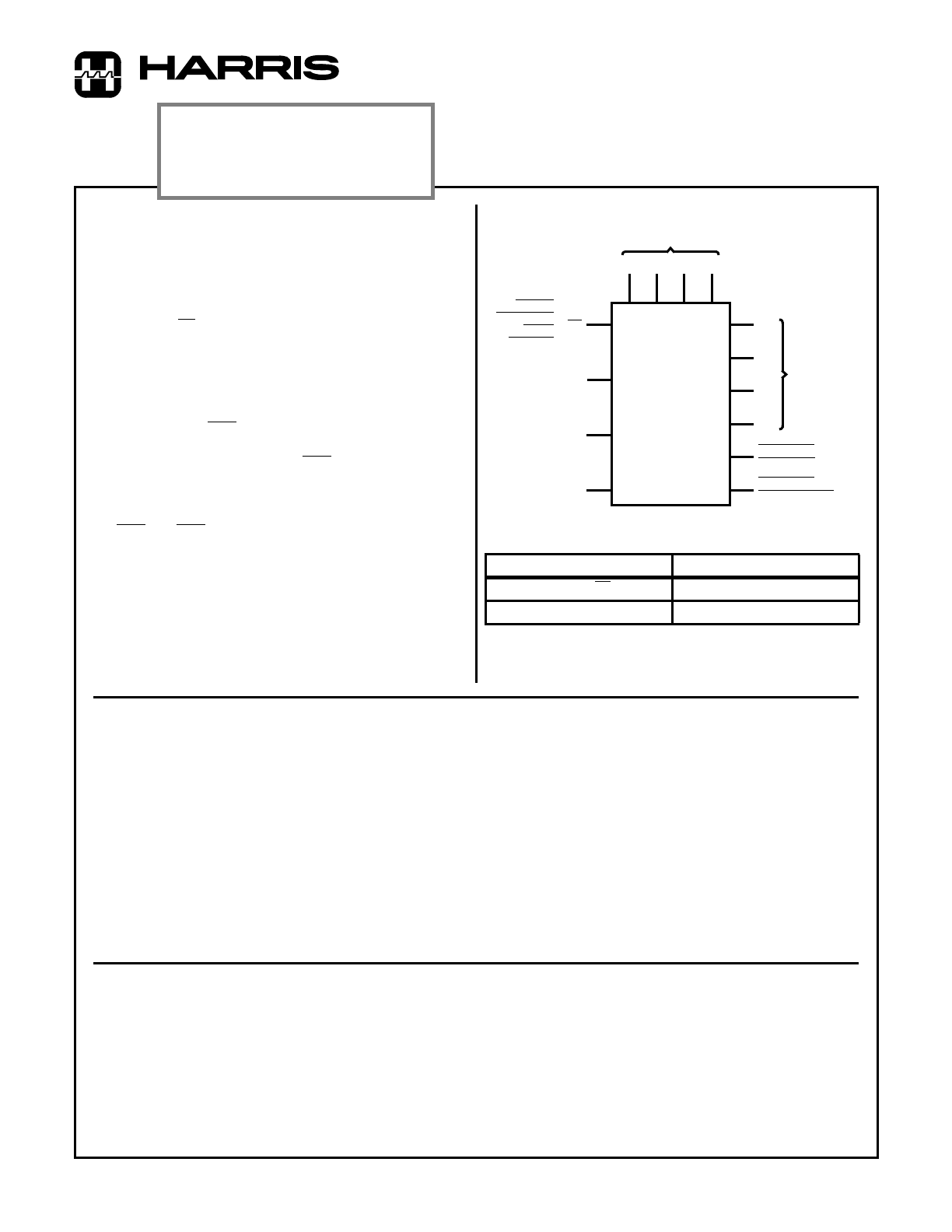
Functional Diagram
ACT INPUT LOAD TABLE
INPUT UNIT LOAD (NOTE 1)
P0 - P3,
PL 0.75
MR, CPU, CPD 0.85
NOTE:
1. Unit load is ∆I
CC
limit specified in DC Electrical Specifications
Table, e.g., 2.4mA Max at +25
o
C.
ASYNC
MASTER
CLOCK UP
11
14
5
15 1 10 9
3
2
6
7
12
Q0
Q1
Q2
Q3
TERMINAL
P0 P1 P2 P3
BINARY PRESET
4 13
COUNT UP
BINARY
OUTPUTS
RESET
CLOCK DOWN
PARALLEL
LOAD
ENABLE
PL
TERMINAL
COUNT DOWN
June 1997
File Number
3897
Description
The CD54AC193/3A and CD54ACT193/3A are up/down
binary counters with separate up/down clocks. These
devices utilize the Harris Advanced CMOS Logic technology.
Presetting the counter to the number on preset data inputs
(P0-P3) is accomplished by a LOW asynchronous parallel
load input (
PL). The counter is incremented on the
LOW-to-HIGH transition of the Clock-Up input (and a HIGH
level on the Clock-Down input) and decremented on the
LOW-to-HIGH transition of the Clock-Down input (and a
HIGH level on the Clock-Up input). A HIGH level on the
Reset input overrides any other input to clear the counter to
its zero state. The
TCU (carry) output goes LOW half a clock
period before the zero count is reached and returns to a
HIGH level at the zero count. The
TCD (borrow) output in the
count down mode likewise goes LOW half a clock period
before the maximum count (15 counts) and returns to HIGH
at the maximum count. Cascading is effected by connecting
the
TCU and TCD outputs of a less significant counter to the
Clock-Up and Clock-Down inputs, respectively, of the next
most significant counter.
The CD54AC193/3A and CD54ACT193/3A are supplied in
16-lead dual-in-line ceramic packages (F suffix).s
Absolute Maximum Ratings
DC Supply Voltage, V
CC
. . . . . . . . . . . . . . . . . . . . . . . . -0.5V to +6V
DC Input Diode Current, I
IK
For V
I
< -0.5V or V
I
> V
CC
+ 0.5V . . . . . . . . . . . . . . . . . . . . . .±20mA
DC Output Diode Current, I
OK
For V
O
< -0.5V or V
O
> V
CC
+ 0.5V. . . . . . . . . . . . . . . . . . . . .±50mA
DC Output Source or Sink Current, Per Output Pin, I
O
For V
O
> -0.5V or V
O
< V
CC
+ 0.5V. . . . . . . . . . . . . . . . . . . . .±50mA
DC V
CC
or GND Current, I
CC
or I
GND
For Up to 4 Outputs Per Device, Add ±25mA For Each
Additional Output . . . . . . . . . . . . . . . . . . . . . . . . . . . . . . . . . . .±100mA
Power Dissipation Per Package, P
D
T
A
= -55
o
C to +100
o
C (Package F) . . . . . . . . . . . . . . . . . . 500mW
T
A
= +100
o
C to +125
o
C (Package F) . . . . . . . . Derate Linearly at
8mW/
o
C to 300mW
Operating Temperature Range, T
A
Package Type F . . . . . . . . . . . . . . . . . . . . . . . . . .-55
o
C to +125
o
C
Storage Temperature, T
STG
. . . . . . . . . . . . . . . . . .-65
o
C to +150
o
C
Lead Temperature (During Soldering)
At Distance 1/16in. ± 1/32in. (1.59mm ± 0.79mm)
From Case For 10s Max . . . . . . . . . . . . . . . . . . . . . . . . . . +265
o
C
Unit Inserted Into a PC Board (Min Thickness 1/16in., 1.59mm)
With Solder Contacting Lead Tips Only. . . . . . . . . . . . . . . +300
o
C
CAUTION: Stresses above those listed in “Absolute Maximum Ratings” may cause permanent damage to the device. This is a stress only rating and operation
of the device at these or any other conditions above those indicated in the operational sections of this specification is not implied.
Recommended Operating Conditions
Supply Voltage Range, V
CC
Unless Otherwise Specified, All Voltages Referenced to GND
T
A
= Full Package Temperature Range
CD54AC Types . . . . . . . . . . . . . . . . . . . . . . . . . . . . . .1.5V to 5.5V
CD54ACT Types . . . . . . . . . . . . . . . . . . . . . . . . . . . . .4.5V to 5.5V
DC Input or Output Voltage, V
I
, V
O
. . . . . . . . . . . . . . . . . . 0V to V
CC
Operating Temperature, T
A
. . . . . . . . . . . . . . . . . . .-55
o
C to +125
o
C
Input Rise and Fall Slew Rate, dt/dv
at 1.5V to 3V (AC Types) . . . . . . . . . . . . . . . . . . . 0ns/V to 50ns/V
at 3.6V to 5.5V (AC Types) . . . . . . . . . . . . . . . . . 0ns/V to 20ns/V
at 4.5V to 5.5V (AC Types) . . . . . . . . . . . . . . . . . 0ns/V to 10ns/V
COMING SOON!
COMPLETE DATA SHEET